Scalable and High-Throughput Top-Down Manufacturing of Optical Metasurfaces
- Journal
- Sensors
- Vol. (No.), pp.
- 20 (15), 4108 (Jul 2020)
- Year
- 2020-2014
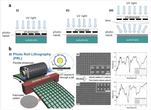
Metasurfaces have shown promising potential to miniaturize existing bulk optical components thanks to their extraordinary optical properties and ultra-thin, small, and lightweight footprints. However, the absence of proper manufacturing methods has been one of the main obstacles preventing the practical application of metasurfaces and commercialization. Although a variety of fabrication techniques have been used to produce optical metasurfaces, there are still no universal scalable and high-throughput manufacturing methods that meet the criteria for large-scale metasurfaces for device/product-level applications. The fundamentals and recent progress of the large area and high-throughput manufacturing methods are discussed with practical device applications. We systematically classify various top-down scalable patterning techniques for optical metasurfaces: firstly, optical and printing methods are categorized and then their conventional and unconventional (emerging/new) techniques are discussed in detail, respectively. In the end of each section, we also introduce the recent developments of metasurfaces realized by the corresponding fabrication methods.


